


Dimensional Measurements of PCB (Printed circuit boad)
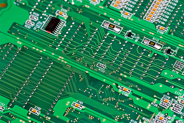
Due to the high-density, multilayer and flexibility of printed circuit boards, a high level of dimensional control is now required in each manufacturing process. In addition, with the proliferation of ISO, quality assurance with established traceability is required, and the demand for reliability in numerical control is increasing.
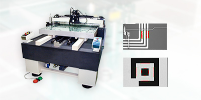
Since Sinto developed the PCB-oriented 2-dimentional coordinate measuring machine in 1990, there have been continuous contributions towards improvements in the level of PCB measurement management.
Pre Process
Measurement of artwork process
Wiring pattern formation is formed via “photolithography” which involves exposing a pattern through original production master . At this stage, measurement is conducted of the film mask that is primarily used as original production master, and of the screen mask that is created by transcription from the film mask.
Measurement Outline
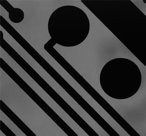
Measurements of Film Masks
The film mask pattern position, line width / space, hole and such like are measured. Via the optional software “C-Auto”, creation of a measurement program based upon the CAD data of the pattern design data is possible, which improves efficiency. Our company’s equipment can be used for the drawing equipment (plotter)
manufacturer’s drawing accuracy evaluation in regard to the drawing of the circuit pattern on the film.
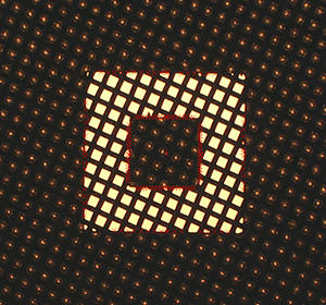
Measurements of Screen Masks
In the screen mask measurement, via image filter functionality and singularity removal functionality, it is possible to conduct accurate measurements that are not influenced by the screen mesh.
Inner・External layer process
Measurement of the wiring pattern formation Process
After copper wiring pattern which formed on the surface of the inner board, the line width / space and position are measured. With the multilayer board, which there are double several pieces internal layer board, every inner layer board are measured.
Measurement of Hole-opening process
Interstitial via hole (IVH*1 ) processed for inner layer connection and through-hole via processed after lamination of all layer are measured.
*1 IVH:Interstitial Via Hole
Measurement Outline
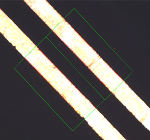
Wiring pattern Measurement
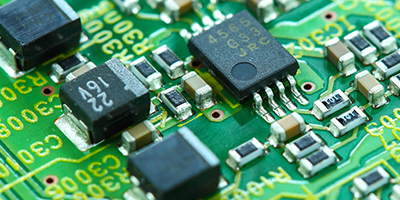
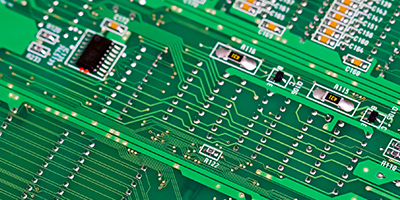
Measures the line width / space and position of the wiring pattern formed on the board. AS ICs or electronic components are mounted on the outer layer board, the position of the surface mount pattern (a pad or land) is also measured.
(Measurement for the position gap of the components mounted by Chip-Mounter is also available.)
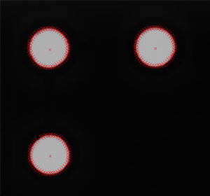
Hole Measurement
The hole and its position that have been opened primarily via drill processing are measured. With the optional software “C-Auto”, based on drill processing NC data, measurement program authoring can be done, and as such work is made more effective. Additionally, our equipment can also be used for precision evaluation of the drilling machine by machine manufacturers.
Post-process
Measurement in Solder resist process
When printing solder on a pad portion where ICs and electronic components are subject to be equipped later, in order to take care not to solder unnecessary parts, the solder resist layer is coated. At this point, the solder resist position to the pad section is measured.
Measurement in Surface processing and Blanking process
Via the screen mask or the metal mask, bumps or solder is printed upon the land/pad portion on which electronic components are equipped. At this point, printing-use mask and the printed solder/bump position are measured. Additionally, after the blanking processing (router rocessing), the board’s outline dimensions are measured.
Measurement in Finished product testing process
Finally, as a pre-shipping inspection, measurements are conducted of the designated areas so as to ensure that the product is finished as per the required specifications of drawing.
Measurement Outline
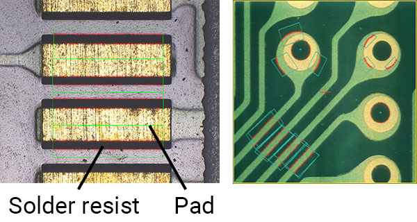
Measurement in Solder resist process
So that malfunctions do not occur when equipping solder-resistant parts to the land/pad section, the solder resist position that is for the land and pad sections is primarily measured. By using the optional color image processing function, the solder resist layer can be confirmed in a clearer image.
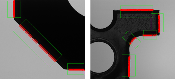
Measurement in Surface processing and Blanking process
As well as measurement of the dimensions and position of the bumps/soldering printed on the land/pad, by using the optional height measurement sensor , height can also be measured. In blanking process, various dimension measurements are conducted after groove and V-groove, hole and other processing.
Measurement in Finished product testing process
At this point, various measurements are conducted, such as external dimension measurement, hole diameter/position, wiring pattern width, and land/pad position.
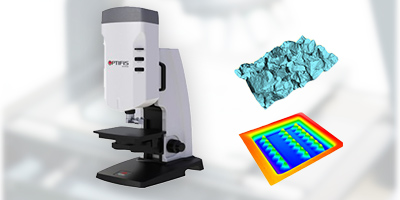
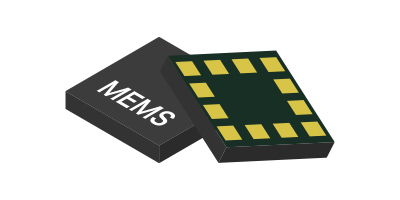
Buildup substrate Measurement
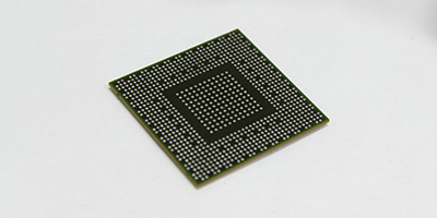
A “buildup substrate” which is built via the formation of multilayers, repeating lamination of each layer to the core board, hole-opening processing, circuit formation, etc. This buildup substrate is more appropriate for high-density than multilayer boards manufactured via conventional processes, and is used for circuit boards that are equipped with LSI, so higher measurement precision is also necessary. Additionally, for connection between the boards, via holes are mainly formed via a laser processor, in which case they are called laser via; the measurement of the laser via is important.
Measurement Outline
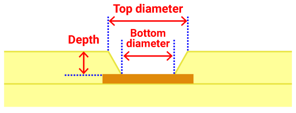
Laser via Measurement
The position/diameter/depth of the laser via that connects directly with the bottommost layer is measured. The depth can be measured via the optional height measurement sensor.
Please consult us for inquiries.
+81-52-581-6896
Available hours: 9:00-12:00 and 13:00-17:00 JST, Monday through Friday
(excluding national and corporate holidays)
![]()